Design for PCB Manufacturing: Five Important Factors for Consideration
Are you planning to design a printed circuit board (PCB) for your next project? Well, there’s more to it than just creating an aesthetically pleasing layout. In fact, there are several factors that you need to consider when designing PCBs for manufacturing. From the type of material used to the size and shape of your board, every detail plays a crucial role in ensuring successful PCB production. To help guide you through this process, we’ve compiled five important factors that you must consider while designing your PCB. So get ready to dive into the world of PCB design and learn everything you need to know about creating efficient and effective boards!
Environmental Factors
When designing PCBs, it is important to consider environmental factors. Five key factors to consider are: material selection, processing, waste management, electrostatic discharge (ESD) protection and final assembly.
Material selection is critical for PCB manufacturers. The type of material used in the PCB will impact the environmental impacts of the manufacturing process and final product. For example, using more environmentally friendly materials can reduce the amount of energy required to produce a PCB and help mitigate environmental impacts associated with production.
Processing is another important factor to consider when designing PCBs. The manufacturing process must be done correctly in order to ensure that the finished product meets all quality requirements and meets or exceeds performance expectations. Improper processing may lead to defects in the finished product that could impact its usability or safety.
Waste management is also important when designing PCBs. Proper waste management practices can reduce environmental impacts associated with production while ensuring that usable materials are recovered and recycled properly.
ESD protection is also important when designing PCBs. Electrostatic discharge (ESD) can damage electronic equipment if it occurs during normal use or during installation or removal of a PCBA from a system. ESD protection products help prevent ESD damage by creating an electrical shield around sensitive devices on a PCB.
Finally, final assembly is an important consideration for PCB designers. Final assembly procedures should be designed so that the finished products meet all functional and quality requirements. Incorrect assembly procedures may lead to defective products
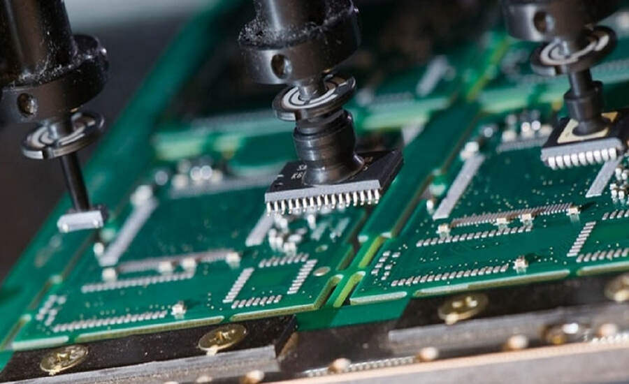
Machine Efficiency
There are a few key factors to consider when designing PCBs for manufacturing. Among these are machine efficiency, yield, part size, routing and plating.
- Machine Efficiency
A key factor in determining the efficiency of a PCB fabrication process is the number of machines used. The more machines that are used, the faster the process can be performed. However, more machines also increase the chances of mistakes being made. It’s important to find a balance between speed and accuracy in order to produce high-quality boards.
- Yield
Another important factor to consider when designing PCBs is yield. Yield refers to how many boards per hour a machine can produce. In order to achieve high yields, it’s important to design your board layout in such a way that as few layers as possible need to be routed on each side of the board. This will reduce the amount of material required for fabrication and result in higher yields.
- Part Size
Part size is another key factor that must be considered when designing PCBs for manufacturing. Too small a part size will increase the amount of time required for routing and plating, while too large a part size will result in increased costs and lower yields. It’s important to use accurate measurements when creating your parts so that they can be manufactured quickly and with minimal errors.
- Routing and Plating
Last but not least, routing and plating are two other important factors that should be taken into account when designing PCBs for manufacturing.
PCB Processing Parameters
PCB processing parameters are important for the design and manufacture of PCBs. In this blog article, we will discuss five important factors for PCB processing: board size, material type, patterning method, solder paste recipe, and reflow profile.
- Board Size
The size of the PCB affects the steps required to create it. For example, a small PCB requires less layers to be printed than a large PCB. The number of leads on the PCB also affects the steps required. Larger boards require more lead widths per inch (LPI) and more lead positions per inch (LPIP).
- Material Type
The material type influences the steps required for manufacturing. For example, a copper PCB requires different processing than a plastic PCB. The material type also affects how heat is transferred during soldering and etching.
- Patterning Method
The patterning method influences the steps required for manufacturing. For example, a silk screen process requires fewer steps than a lithography process. The patterning method also affects how heat is transferred during soldering and etching.
- Solder Paste Recipe
The solder paste recipe influences the steps required for manufacturing. For example, a low-melting-point solder paste recipe reduces the number of thermal cycle requirements during assembly operations
PCB Design Guidelines
Design for PCB Manufacturing: Five Important Factors for Consideration
PCB design is an important process in the manufacturing of electronic devices. It can be difficult to get the correct dimensions and layout of the circuit board, which can lead to errors in component placement and overall device quality. Here are five important factors to consider when designing a PCB:
1. Layout flexibility
Layout flexibility is one of the most important factors to consider when designing a PCB. The layout should be able to accommodate future changes without requiring significant modifications or rework. This means that you should allow for a variety of component placements and routing options.
2. Component placement accuracy
Component placement accuracy is also crucial when designing a PCB. Not all components will fit perfectly on the board, which can lead to short circuits or other malfunctions. Keep track of component spacing and make sure that all pins and pads are big enough to accommodate them without issue.
3. Component orientation accuracy
Some components require specific orientations in order to function properly, so it’s important to ensure that your boards are laid out accurately in preparation for assembly. Orientation errors can cause problems with signal flow and device operation.
4. Signal integrity
Even though your PCB design may be perfect from a layout standpoint, if there are any problems with signal integrity, they will still manifest themselves as defects during production processes like soldering and coating. Make sure that all signals run smoothly through your board without any
Conclusion
In order to create PCB designs that are both manufacturable and compliant with industry standards, manufacturers must carefully consider a variety of factors. This article highlights five key areas that should be considered when designing for PCB manufacturing. By understanding these considerations and incorporating them into your design process, you can ensure that your final product is reliable and meets the needs of the market.